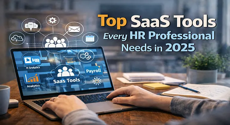
Top SaaS Tools Every HR Professional Needs in 2025
As an HR professional, I understand the challenges that come with the job. There are long, difficult hours spent on recruitment, payroll processing, onboarding, engagement, performance reviews (and reviewing performance), and managing employees in the new hybrid working model. The role of HR has changed. Today’s HR professionals are not focusing on managing paperwork; they are driving positive change in the workplace and generating bottom-line results for the company.
Modern SaaS tools are really starting to help. Today’s tools are improving the way we analyze our work and allowing HR professionals to spend valuable time on the employees.
Modern time tracking software like Controlio provides valuable insight on employee engagement. It’s especially useful for “overseeing” remote employees.
Based on my conversations with transformed HR leaders, the following are the 15 best SaaS tools for HR professionals in 2025. My selections are based on trends and reviews.
Controlio
Controlio is a …
Top SaaS Tools Every HR Professional Needs in 2025 Read More