
Semiconductor wafers are the foundation of every modern electronic device, but producing them at high yield requires a relentless focus on precision. Even the most minor nanoscale flaws can compromise functionality, reducing performance or rendering chips unusable. Traditional inspection methods, while advanced, are reaching their limits as circuit patterns shrink to near-atomic dimensions. Erik Hosler, a semiconductor innovation expert, highlights how AI-powered inspection systems are setting new standards for precision in fabrication. Artificial intelligence is now reshaping wafer inspection through enhanced imaging, combining optical and electron microscopy with machine learning to identify once undetectable defects.
This shift is arriving at a crucial time for the industry. The demand for smaller, faster, and more efficient chips continues to grow across sectors such as artificial intelligence, automotive, and mobile devices. Meeting this demand requires manufacturers to eliminate waste and maximize yields while pushing the boundaries of miniaturization. AI-enhanced imaging offers a path forward by augmenting human expertise with computational accuracy, enabling fabs to detect, classify, and correct flaws at unprecedented scales.
The High Stakes of Wafer Inspection
Wafer inspection is among the most critical steps in semiconductor manufacturing. A single undetected defect can propagate through later stages of production, magnifying costs and reducing yields. As chips shrink to nodes measured in nanometers, the challenge of identifying such defects becomes exponentially more complicated.
Traditional optical systems can detect larger anomalies but struggle with the sub-nanometer irregularities that matter most in advanced processes. Electron microscopy offers higher resolution, yet it is slow and resource-intensive, making it impractical for inspecting every wafer at scale. Manufacturers need inspection methods that combine the accuracy of electron microscopy with the efficiency of optical systems, something AI makes possible.
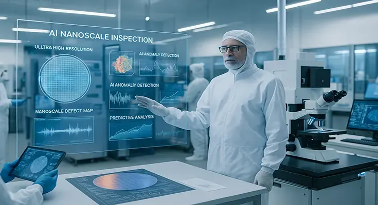
How AI Enhances Imaging
AI-driven imaging transforms inspection by automating the analysis of data collected from advanced microscopes. Machine learning models trained on vast datasets of wafer images can distinguish between harmless variations and defects that impact performance. This capability reduces false positives, saving time and resources while focusing attention on the issues that matter most.
More importantly, AI can detect patterns invisible to human operators. By learning from millions of images, AI systems develop the ability to recognize faint signatures of potential defects before they develop critical problems. This predictive power turns inspection into a proactive process, reducing rework and improving yield.
Beyond Human Limits
The complexity of nanoscale inspection makes AI an invaluable complement to human expertise. Human operators are skilled at identifying known patterns but may overlook anomalies that do not fit expected categories. AI expands the horizon of detection by analyzing data at speeds and scales impossible for people to match.
This synergy between human judgment and AI-driven insight creates a more comprehensive inspection system. Engineers can focus on interpreting the context of anomalies while AI handles the exhaustive task of scanning and categorizing data. The result is a more reliable and efficient inspection process.
Precision at the Sub-Nanometer Scale
One of the most significant breakthroughs enabled by AI-enhanced imaging is precision at the sub-nanometer level. Advanced imaging tools combined with machine learning allow fabs to resolve features smaller than the wavelength of visible light.
Erik Hosler emphasizes, “Free-electron lasers are revolutionizing defect detection by offering unprecedented accuracy at the sub-nanometer scale.” His insight underscores how AI-integrated imaging tools are unlocking new levels of precision that redefine the limits of inspection.
This advancement is not just about seeing more minor details, but transforming inspection into a predictive science. With sub-nanometer precision, fabs can understand defect formation mechanisms, improve process control, and design countermeasures before flaws affect yield.
Transforming Yield Management
AI-enhanced imaging directly impacts yield management by reducing waste and improving throughput. By catching defects earlier and more accurately, fabs can minimize the number of wafers scrapped due to undetected flaws. Improved classification also ensures that minor, non-impactful variations do not trigger unnecessary corrective actions, saving both time and resources.
For manufacturers, these improvements translate into higher productivity and lower costs. In an industry where profit margins often hinge on yield percentages, the ability to improve inspection outcomes can even have massive financial implications.
Applications Across Industries
The benefits of AI-driven wafer inspection ripple across multiple industries. In automotive, where chips must meet stringent safety and reliability standards, enhanced imaging ensures consistent quality. In consumer electronics, it enables faster innovation cycles by reducing the risk of defects delaying product launches.
Yield improvements translate directly into meeting global demand in data centers and AI infrastructure, where massive chip volumes are required. Furthermore, research in quantum computing stands to benefit, as qubits require defect-free environments that only the most advanced inspection systems can ensure.
Challenges of Implementation
Despite its promise, implementing AI-enhanced imaging in fabs presents challenges. Training machine learning models requires enormous amounts of high-quality data, and collecting these datasets can be costly and time-consuming. Integrating AI with legacy inspection systems also demands significant investment in infrastructure and expertise.
Another concern is interpretability. Engineers must be able to trust AI decisions and understand why defects are classified in specific ways. Developing explainable AI systems is critical to ensuring adoption and building confidence in the technology. Finally, as imaging systems become more powerful, data storage and processing requirements escalate, creating additional challenges for fabs already handling petabytes of information.
Seeing the Future of Semiconductor Precision
AI-enhanced imaging is redefining wafer inspection by pushing the boundaries of precision, speed, and predictability. By combining optical and electron microscopy with machine learning, fabs can now identify nanoscale flaws before they compromise yield. The shift from reactive defect detection to predictive, AI-driven inspection marks a fundamental leap in manufacturing capability.
As demand for high-performance chips accelerates, fabs that embrace these technologies will set the standard for quality and efficiency. AI-driven imaging does more than improve inspection. It reimagines it, creating a future where defects are not just found but anticipated and prevented. In this new vision of semiconductor manufacturing, precision is no longer a goal to strive for, but a constant, achievable reality.